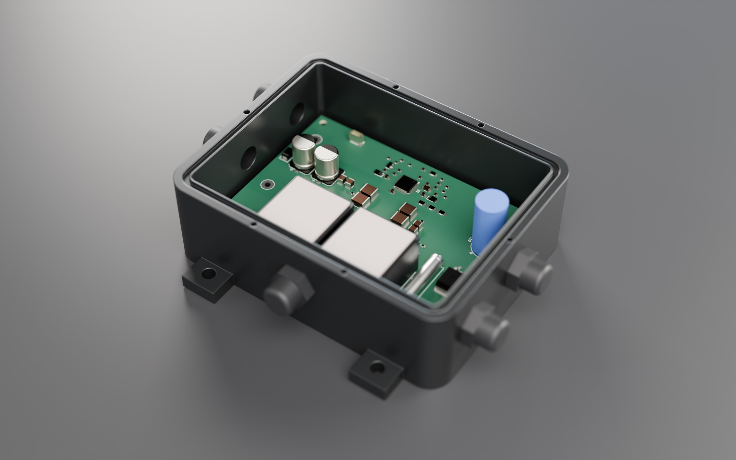
Day three of the Hyperscooter — a scooter we are designing from scratch: our own frame, our own suspension, our own controllers. On this day it got the module that will power everything on board except the motors: headlights, lights, horn, a phone socket and the head unit on the handlebar. This entry is how we designed it and what we know about it so far — from calculation only.
How much is needed
We started with the list of loads. The biggest one is not the headlights but the USB-C PD socket for a phone and a laptop.
| Load | Power | Current at 12 V |
|---|---|---|
| Headlights, 2 pcs | 35–40 W each | 5.8–6.7 A |
| USB-C PD socket | 100 W | ~9 Avia its own PD converter, ~92 % efficiency — estimate |
| Horn, automotive | — | 3–5 A, briefly |
| Tail light, brake light, indicators | 10–20 Westimate | ~1.5 A |
| Head unit | 5–10 Westimate | ~1 A |
| All at once | ~280 W | ~23 A |
We sized the module for 25 A at 12 V, which is 300 W: with headroom for a pump and fans, should they be needed.
And one more condition on top: one module for two scooters. The Ninebot G30 has a 16S battery, the big one has 24S. So the input spans from an empty 16S to a full 24S with regenerative braking.
Why 150 volts
Regenerative braking on the big scooter can push the bus up to 115 V — the cut-off we proposed for the controllers. And the switch node rings above the input on every cycle, by 10–20 V even with a good layout (estimate).
A 120 V part leaves 5 V of margin above regen — less than the ringing. We need the 150 V class: then 35 V are left for ringing.
We took the ADI LTC7810: input up to 140 V, 150 V absolute maximum, two channels that can be combined into two phases driving one output. Its datasheet has a reference design that is almost our task — 12 V / 30 A from 8–140 V — and that is where we started.
A reference design is not a finished design
Two phases shifted by 180° split the current in half: less ripple at the input and output, and the heat is spread over four MOSFETs and two inductors.
We did not copy the ADI reference design one to one: in four places it does not fit us.
| Part | Reference design | Ours | Why |
|---|---|---|---|
| MOSFETs | BSC190N15NS3, 2 in parallel | BSC093N15NS5, single | diode reverse recovery charge 385 → 58 nC |
| Inductor | XAL1510-103 | SER2918H-103KL | the XAL1510 series is rated 60 V |
| Bootstrap | 0.1 µF | 0.47 µF | the datasheet's own rule: ≥ 100 × MOSFET Ciss |
| Output polymer | 16 V | 25 V | at 12 V the margin was only ×1.33 |
With the original MOSFETs, diode recovery at 115 V would cost ~8.9 W on each low-side switch. ADI uses the BSC093N15NS5 in another of its reference designs, for inputs up to 140 V.
Losses
We calculated losses with the equations from the LTC7810 datasheet, MOSFETs hot. MOSFET output charge and diode recovery are taken with a margin on the high side.
| Input | Loss | Efficiency | Battery current |
|---|---|---|---|
| 48 V16S empty | 10.8 W | 96.5 % | 6.5 A |
| 67.2 V16S full | 12.5 W | 96.0 % | 4.6 A |
| 100.8 V24S full | 15.8 W | 95.0 % | 3.1 A |
| 115 Vregen | 17.4 W | 94.5 % | 2.8 A |
The higher the input, the more heat: the voltage-dependent losses grow — high-side switching, recharging its capacitance, diode recovery. The hottest spots are the low-side MOSFETs: each takes about a quarter of the module's total loss.
Protection
The module has no microcontroller of its own, so everything it does in a fault is done in hardware.
| Event | Module | Recovery |
|---|---|---|
| Input below 32.4 V | stops switching | automatic, above 35.9 V |
| Input above 125.5 V | stops switching | automatic, below 118.8 V |
| Output short circuit | current limit folds back to 40 %, ~16 A average | automatic |
| High-side MOSFET fails short | at 13.2 V turns the low-side on, current goes through the fuse; the low-side most likely dies too | replace both MOSFETs of the phase and the fuse |
| Battery wires swapped | diode conducts, fuse blows | replace fuse |
| Spike on 12 V | SMBJ15A TVS | — |
The board: reworked by the checklist
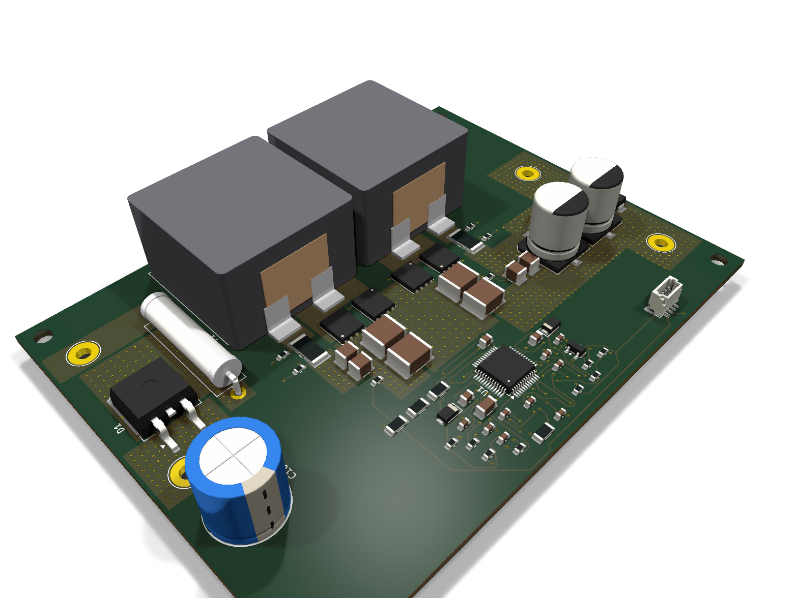
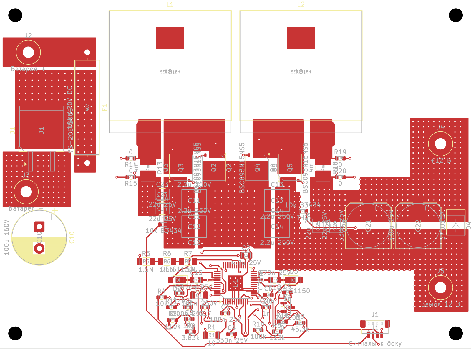
The board is 108 × 80 mm, 4 layers. Schematic and board are generated by Python scripts in KiCad, signal traces are routed by Freerouting, power copper and tricky connections by our own script.
The first placement looked neat: each phase under its own inductor, everything symmetrical. An outside reviewer sent comments on the layout, we re-read the checklist at the end of the datasheet — and found we broke its very first item.
Heat: the calculation found the problem before the order
The module lives in a sealed enclosure: IPX9K and IPX7, no fan. Heat leaves through the floor into the aluminium plate of the frame.

You cannot get this from a single watts-to-degrees number, so we built a model from the board's actual copper: a 0.5 mm grid over four layers, copper conducts only within its own net, and between layers there is fibreglass and via walls.
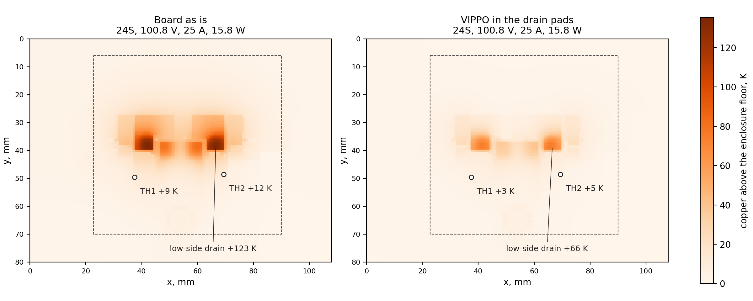
| Option | Above floor |
|---|---|
| As is | +127 K |
| Vias next to the pad | +135 Kworse: cut-outs in the planes |
| 150 kHz instead of 200 | +111 K |
| VIPPO in the drain pads+ switch node on the bottom layer | +70 K |
| VIPPO and 150 kHz | +61 K |
| VIPPO, 150 kHz, 70 µm copper | +56 K |
Vias next to the MOSFET do not help: heat does not reach them through thin copper. Only vias right in the drain pad, filled and capped with copper — VIPPO — do. We are finding out what the board house charges for it; the decision for Rev A is still open.
The dock handles overheating
Each phase has an NTC sensor next to the low-side MOSFET, both routed to the connector. The module itself does not know which load matters more — the dock of the head unit on the handlebar does. It reads the temperature, reports it to diagnostics and sheds load in steps.
| Copper at the MOSFET | What the dock turns off |
|---|---|
| 95 °C | the USB-C PD socket |
| 105 °C | spare loads; the horn — briefly only |
| 115 °C | everything except lightsheadlights, tail light, brake light and indicators stay on |
The lights are never turned off — the owner's decision: on the move they matter more than an intact board. With only the lights on, the module delivers ~90 W and loses almost half as much as at full load.
How much of this is true
We asked ourselves this before publishing. The answer differs from number to number.
| What | Source | Trust |
|---|---|---|
| Input thresholds, current limit, 12 V output | datasheets and arithmetic | solid |
| Losses and efficiency | first-order model | ±20–30 % |
| Heating | model from the board copper | direction yes, degrees ±tens |
| Ripple, ringing, stability, crowbar vs battery | not calculated | bench only |
The next entry about the module will come from the bench: efficiency at several points, a thermocouple on the low-side MOSFET, a scope trace of the switch node at 115 V, and a comparison with this article — where we were right and where we were not.
What exists now
- Rev A schematic and board: KiCad checks pass clean, 58 parts.
- Loss calculation and the thermal model from the board copper — as scripts, recalculated on every board change.
- Enclosure sketch: a machined aluminium tub, floor down on the frame plate.
- A module datasheet and a schematic description for review.